1 / 3
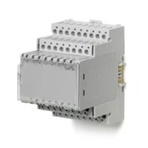
A professional PCBA supplier offers one-stop electronic manufacturing solutions covering ODM/OEM, multilayer PCB fabrication, PCBA assembly, and custom software development. Below is a detailed breakdown of core capabilities, technical specifications, and service advantages.
| Specification Category | Specification Item | Detailed Description |
|---|---|---|
| Core Service Scope | ODM/OEM Services | End-to-end customization: From product conceptual design, schematic layout, PCB design to prototype trial, mass production, and after-sales support. Supports full-system customization (hardware + software integration). |
| Multilayer PCB Fabrication | Layer count: 1 - 48 layers (common: 4 - 16 layers for industrial/consumer electronics); Customizable for high-frequency, high-Tg, halogen-free, and flexible PCB requirements. | |
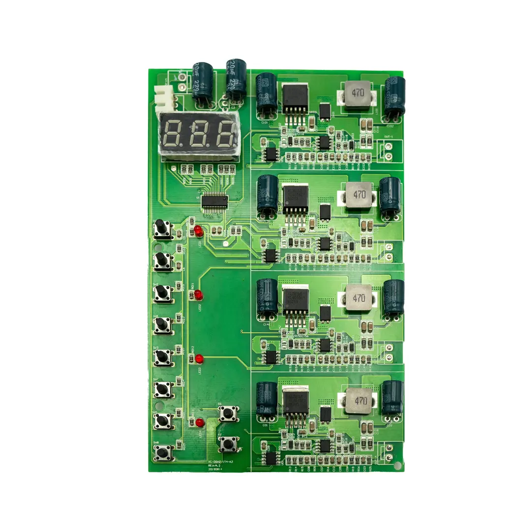
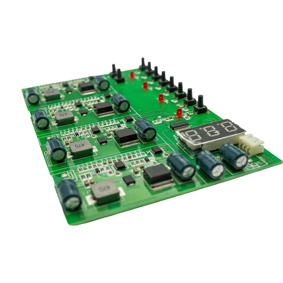
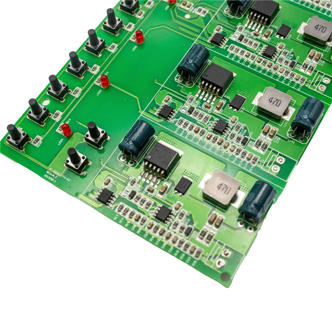
| PCBA Assembly | Combined SMT + THT assembly; Supports ultra-fine-pitch components (BGA, QFP, 01005 chips) and large-size PCBA (max. 600mm × 800mm). | |
| Custom Software/App Development | Embedded firmware (MCU/ARM/Intel platform), IoT application software, industrial control system software, mobile APP (iOS/Android) and desktop software development. | |
| PCB Fabrication Specifications | Minimum Line Width/Spacing | 2/2 mil (0.051mm/0.051mm) for standard boards; 1/1 mil (0.025mm/0.025mm) for high-precision boards. |
| PCB Thickness Range | 0.1mm - 10.0mm; Common specifications: 0.8mm, 1.0mm, 1.6mm (compliant with IPC-6012). | |
| Substrate Material | FR-4 (standard), High-Tg FR-4 (Tg ≥ 170°C), Rogers (high-frequency), PI (flexible), halogen-free materials (compliant with IEC 61249-2-21). | |
| Surface Finish | HASL (lead-free), ENIG (Electroless Nickel Immersion Gold), OSP (Organic Solderability Preservative), Immersion Silver/Tin, Hard Gold Plating. | |
| PCBA Assembly Specifications | Component Placement Accuracy | Chip components: ±0.03mm; Fine-pitch ICs (≤0.4mm pitch): ±0.02mm; BGA/CSP: ±0.015mm (Yamaha/Juki high-speed placement machines). |
| Soldering Standard | Lead-free soldering (compliant with RoHS 2.0); Nitrogen reflow soldering (optional, oxygen content ≤500ppm); Solder joint voiding rate: <5% (BGA/CSP, tested by X-Ray). | |
| Assembly Testing Process | SPI (Solder Paste Inspection) → AOI (Automatic Optical Inspection) → X-Ray (for BGA/CSP) → ICT (In-Circuit Test) → Functional Test (FCT) → Burn-in Test (optional for industrial products). | |
| Software Development Capabilities | Supported Platforms | Embedded: STM32, Arduino, Raspberry Pi, Intel x86, ARM Cortex; Mobile: iOS (Swift/Objective-C), Android (Kotlin/Java); IoT: MQTT, CoAP, LoRaWAN, NB-IoT protocols. |
| Development Deliverables | Source code, technical documentation (API manual, user manual), test reports, and 1-year free bug fixes. | |
| Production & Quality Assurance | MOQ (Minimum Order Quantity) | Prototype: 1 PCS; Small-batch: 10 - 200 PCS; Mass production: ≥200 PCS (flexible for customized projects). |
| Production Lead Time | Prototype: 3 - 7 workdays; Small-batch: 10 - 15 workdays; Mass production: 15 - 30 workdays (subject to BOM procurement status). | |
| Quality Certifications | ISO 9001, IPC-A-610 (Class 2/3), IPC-6012, RoHS 2.0, REACH; Medical electronics: ISO 13485 (optional). | |
| Defect Rate Guarantee | PCBA pass rate ≥99.5% (initial inspection); Solder joint defect rate <0.1% (compliant with IPC-A-610 Class 2). | |
| Supply Chain & Logistics | Component Sourcing | Global supplier network (Digikey, Mouser, AVNET); BOM optimization & cost reduction; Anti-counterfeit verification (X-Ray, laser marking inspection). |
| Logistics Services | Global delivery via DHL/FedEx/UPS; Customs clearance assistance; Batch shipment & inventory management (optional). | |
| Value-Added Services | DFM/DFA Analysis | Pre-production design review to optimize manufacturability, reduce costs, and avoid assembly risks (free for bulk orders). |
| After-Sales Support | 12-month warranty for PCBA products; Technical consultation (24-hour response for urgent issues); On-site debugging support (optional for large projects). |

We support the fabrication of multilayer PCBs ranging from 1 to 48 layers. Common configurations for industrial and consumer electronics typically feature 4 to 16 layers, utilizing customizable high-frequency, high-Tg, halogen-free, and flexible materials.
Prototype fabrication is typically completed within 3 to 7 workdays (expedited 24-hour sampling is available). Small-batch trial production takes 10 to 15 workdays, while mass production requires 15 to 30 workdays, depending on component BOM procurement status.
Yes. Our SMT lines feature high-speed Yamaha and Juki placement machines that easily support ultra-fine-pitch components, including BGAs/CSPs and ultra-micro 01005 chip components with placement accuracy down to ±0.015mm.
We strictly adhere to the IPC-A-610 (Class 2/3) standard. We perform a multi-stage verification process including Solder Paste Inspection (SPI), Automatic Optical Inspection (AOI), X-Ray inspection for BGA/CSP hidden solder joints, In-Circuit Testing (ICT), and Functional Testing (FCT) to guarantee a solder joint voiding rate under 5%.
We offer flexible MOQs depending on the stage of your project. The MOQ for standard prototypes is 1 PCS, small-batch trial runs are typically 10 to 200 PCS, and full mass production starts from 200 PCS.
Yes, we provide comprehensive Design for Manufacturability (DFM) and Design for Assembly (DFA) optimization reviews before launching production. This process helps identify potential layout risks, reduces production costs, and is free for bulk orders.