1 / 2
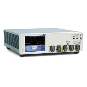
The Keysight 4881HV is a specialized high-voltage (HV) wafer-level test system designed to address the testing needs of high-voltage semiconductor devices—such as power management ICs (PMICs), discrete power components (e.g., MOSFETs, IGBTs), and high-voltage sensors—during wafer fabrication and characterization phases. It integrates precise high-voltage sourcing, measurement capabilities, and wafer-handling compatibility to enable efficient, reliable testing of devices operating at elevated voltage levels, while ensuring accuracy and compliance with industry standards.
The system is tailored for testing high-voltage semiconductor devices across multiple stages of the production and R&D workflow, including:
| Specification Category | Details |
|---|---|
| Core Functionality | Specialized high-voltage (HV) wafer-level test system for characterization, production testing, and R&D of high-voltage semiconductor devices (e.g., PMICs, power MOSFETs, IGBTs, HV sensors). |
| Voltage Sourcing & Measurement Range |
• Sourcing Voltage: Up to 1000 V DC (configurable based on module; optional extensions for higher voltage needs). • Measurement Voltage: Compatible with DC voltage measurements up to 1000 V (matches sourcing range for consistency). |
| Current Measurement Capability |
• Range: Supports sensitive current detection down to nA (nanoampere) to µA (microampere) levels (critical for measuring leakage currents in HV devices). • Accuracy: Typical ±0.1% of reading (varies by current range and operating conditions). |
| Wafer Compatibility |
• Wafer Sizes: Supports standard semiconductor wafer diameters: 6-inch (150 mm), 8-inch (200 mm), 12-inch (300 mm). • Probe Card Integration: Compatible with high-voltage probe cards (e.g., Kelvin probe cards for low-resistance measurements) and automated wafer prober interfaces. |
| Safety Features |
• Overvoltage Protection (OVP): Programmable OVP limits to prevent device/system damage. • Overcurrent Protection (OCP): Adjustable OCP thresholds for current surge mitigation. • Safety Interlocks: Physical interlocked enclosures and emergency stop (E-stop) function (compliant with IEC 61010 safety standards). • HV Alert Indicators: Visual/audio alarms for high-voltage activation. |
| Hardware Architecture |
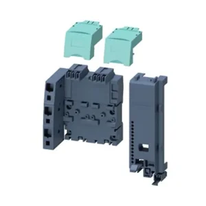
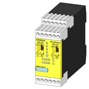
• Modular Design: Configurable with high-voltage Source-Measure Units (SMUs), control modules, and prober interface cards. • Channel Count: Scalable channel options (typically 4–16 channels, expandable based on test requirements). • Control Unit: Embedded processor for test sequence management and data processing. |
| Software Compatibility |
• Test Automation: Supports PathWave Test Executive, VEE Pro, and LabVIEW for custom test sequence creation. • Data Management: Real-time data logging, pass/fail analysis, and integration with enterprise MES (Manufacturing Execution Systems) for traceability. |
| Operating Environment |
• Temperature Range: 15 °C – 35 °C (operating); 0 °C – 55 °C (storage). • Humidity Range: 20% – 80% RH (non-condensing). • Power Supply: 100 V AC – 240 V AC, 50/60 Hz (single-phase). |
| Key Industry Applications | Automotive (EV/HEV power devices), industrial (motor drives, renewable energy inverters), consumer electronics (HV chargers/ICs), and semiconductor R&D (high-voltage device design validation). |
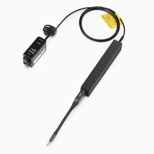
A variety of MMIC amplifiers are available, ideal for microwave radio, aerospace and defense, and instrumentation applications.
Delivery information typically includes delivery times, shipping methods, packaging, etc., which may vary depending on the seller and the location of purchase.